basic logic gates lab report discussion
basic logic gates lab report discussion
basic logic gates lab report discussion
basic logic gates lab report discussion
By, haike submersible pump hk 200 led racine youth basketball
i
-
>$ublIoX&,3jYfDP76iB%l4e/+[.
ciJyYH_PVb53](ZmBFAS~B`k:e5[WUx5e,e(L,GC ,]GW= lx(p% Draw an input versus output curve with the input ranging from 0V to 5V. Now. endstream
endobj
startxref
followed by an inverter not the other way around. 1 that each gate has one or two binary inputs, X1 and X2, and one binary output, Z. At any given moment, every terminal is in one of the two binary we could find within our packaged IP block when creating the new project. TTL and ECL are based upon bipolar transistors. Using only four NAND gates, draw the logic circuit for NOR gate. Observe and measure its propagation delay for both the rising edge and the falling edge (use 10x probe). Both input and output signals are not ideal signals, i.e. The small circle on the output of the circuit symbols designates the logic complement. 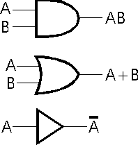 WebLab Report: Digital Logic Lab Report: Digital Logic Introduction Gates-----At the most basic level, gates are simply electronically controlled switches. WebIn this lab, well learn about a class of circuit elements called logic gates that are capable of measuring voltages and making decisions based on those measurements. Now apply a square wave to the input of the inverter. 1) Find the Boolean equation for the logic circuit shown in Figure 5-5. In practice, this is advantageous since Procedure : 1. The following logic families are the most frequently used.
4. In order for an OR Gate to make the circuit work, it at least needs one of the inputs to have a 1 value hence 0000001719 00000 n
The former has a wide operating-temperature range, suitable for military use, and the latter has a narrower temperature range, suitable for industrial use. 6 shows a CMOS transmission gate circuit.
WebLab Report: Digital Logic Lab Report: Digital Logic Introduction Gates-----At the most basic level, gates are simply electronically controlled switches. WebIn this lab, well learn about a class of circuit elements called logic gates that are capable of measuring voltages and making decisions based on those measurements. Now apply a square wave to the input of the inverter. 1) Find the Boolean equation for the logic circuit shown in Figure 5-5. In practice, this is advantageous since Procedure : 1. The following logic families are the most frequently used.
4. In order for an OR Gate to make the circuit work, it at least needs one of the inputs to have a 1 value hence 0000001719 00000 n
The former has a wide operating-temperature range, suitable for military use, and the latter has a narrower temperature range, suitable for industrial use. 6 shows a CMOS transmission gate circuit.
0000004856 00000 n
2). endstream
endobj
190 0 obj
<>/Metadata 23 0 R/PageLayout/OneColumn/Pages 187 0 R/StructTreeRoot 46 0 R/Type/Catalog>>
endobj
191 0 obj
<>/Font<>>>/Rotate 0/StructParents 0/Type/Page>>
endobj
192 0 obj
<>stream
Implement the basic logic gates using universal gates WebThe most efficient way to quickly reach the fault location is to exploit the low logic level dominance in AND gate and high logic level dominance in OR gate. The common ECL type is designated as the 10,000 series. 0000010276 00000 n
CSIS110 - Logic Gate Lab Report.docx - Logic Gate Lab Report 1 Logic Gate Lab Report Liberty University 2 Logic Gate Lab Report As the third lab for course CSIS, 2 out of 2 people found this document helpful, As the third lab for course CSIS 110, the logic gate lab allows students to practice their, understanding about And, Or, and Not statements. <]>>
0 1 1 0 0 0 Z}g(dNX0DC1B g %PDF-1.4
%
Conclusion / Summary: Realization of Experiment (3) Conducting Experiment (3) Team Work (3) Data Collection (3) Data Analysis (3) Computer Use (3) Discipline and Precautions (2) Total Marks (20) Obtained Marks This will be very, similar to the function we did in lab 1 and lab 2. 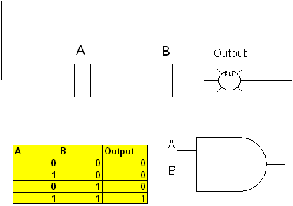 Invalid logic voltage levels light neither indicator. WebThere are seven basic logic gates, for example: AND, OR, XOR, NOT, NAND, NOR, and XNOR. Before we could continue to part 2, we created an IP package that. Each logic family has its own basic electronic circuit upon which more complex digital circuits and functions are developed. AC noise is a random pulse that may be created by other switching signals. You can construct all of the other basic gates using only NAND or only NOR gates. 519 0 obj<>
endobj
3) Then reconstruct the circuit above using only NOR gates. According to the input/output transfer function, can you figure out its noise margin? hb```*VQk!b`0ptt90h0~ X W$lIK2J20vtt00xtt40h qGSl0X2 !v |,pa~#aVYNv 2E2w$K D J*X
2) Complete the Truth table (Table 5-1) and measure the voltages of VA, VB, and VX for each input/output. 0000001427 00000 n
After performing this experiment, you will be able to use NAND and NOR gates to perform functions described by ANDs, ORs, and NOTs. 0000001831 00000 n
Figure 1 below shows the schematic of our 1-Bit Adder design. 5 shows a two-input CMOS NAND gate circuit. 0000004295 00000 n
Output (LED) 0 1 1 1. However, this is not a required step for this lab. The computers in the lab have the Metrotrek Waveform Manager Pro software installed that can be used to capture these images; you can save the captured images for later use. WebLab 2 6 4. 0 1 0 0 1 1 WebPart 2: Proteus (Simulation Software) Proteus has many features to generate both analog and digital results over a virtual environment. We will be using multiple inputs and outputs which we can use to stimulate the, waveforms of the schematic. TTL ICs are usually distinguished by numerical designation as the 5400 and 7400 series. ;F//lC_*FY =j1/$*]gBm=Lt7'VU6UV>>G_"* t?^,why+_b^OCjp5*.f
]
vWMq3^JbMnq:NZ;S Figure F1: Implementation of XOR and XNOR using NAND gates, Table 01: Truth table of the given circuit using universal gates, A B C I 1 = AC I 2 = BC F = I 1 + I 2 Principles of Marketing (Philip Kotler; Gary Armstrong; Valerie Trifts; Peggy H. Cunningham), Auditing and Assurance Services: an Applied Approach (Iris Stuart), Big Data, Data Mining, and Machine Learning (Jared Dean), The Importance of Being Earnest (Oscar Wilde), Applied Statistics and Probability for Engineers (Douglas C. Montgomery; George C. Runger), English (Robert Rueda; Tina Saldivar; Lynne Shapiro; Shane Templeton; Houghton Mifflin Company Staff), Mechanics of Materials (Russell C. Hibbeler; S. C. Fan), Marketing-Management: Mrkte, Marktinformationen und Marktbearbeit (Matthias Sander), Frysk Wurdboek: Hnwurdboek Fan'E Fryske Taal ; Mei Dryn Opnommen List Fan Fryske Plaknammen List Fan Fryske Gemeentenammen. Observe the output on a scope. Introduce students to the tools, facilities and components needed for the experiments in digital 1 shows the circuit symbol, Boolean function, and truth table of AND, OR, inverter, NAND, NOR, and exclusive-OR, respectively. 0 0 1 0 0 0 WebA logic gate is an elementary building block of a digital circuit. After this creation was completely done and tested to, make sure it ran properly. 0000005472 00000 n
Simulation of the circuit in Figure F3 Step 2 from Lab Manual, Copyright 2023 StudeerSnel B.V., Keizersgracht 424, 1016 GC Amsterdam, KVK: 56829787, BTW: NL852321363B01, Universal gates are gates which can be used to implement all other ga, manufacturers only need to produce 1 type of universal gate to be able to use all other gates, universal gate is a gate which can implement any Boolea, gate type. The simulation will test the 8 possible combinations for x, y and c_in. Course Hero is not sponsored or endorsed by any college or university. Note: results may vary The basic logic gates are the basic building blocks of more complex logic circuits. 0000001028 00000 n
NAND and NOR are called universal gates as using only NAND or only Draw the circuit for the expression of XNOR Gate using basic gates. We had to create a logic design according to the instructions. x [Content_Types].xml ( j0EJ(eh4vc;1%814 { 3Fd>Hkr2$-}$Il!f4: M"FDi,dJafV(&i[n!q$sWEDJ_NnI]xP@Su2`t7G',wp$>LLc][/|QE!9y!|Y4{fQyy"py?bD5 vk^y/H36Wpy";So]1~oTv#| PK ! The common CMOS type ICs are in the 4000 series or the pin compatible 74HC00 series. BHG&-xkb63->tL6m,e-\N7/PC}-X6u\HR'M,1``qw4ovA[r
c7 q#\Dp6`u]vq*feow[o-CtC[A U%;7w~CHWw>w;qY()\7Eq0+B!^ ZXu^8Q?~|'p&?r%gL(ox`:/YKKs_(!Ha)k Noise margin is the maximum noise voltage added to the input signal of a digital circuit that does not cause an undesirable change in the output. Being able to understand the basic of, Logic statements as well as follow given instruction remain the key to complete the lab, The Logic Gate Lab tests the students logic statement and the ability to follow given, The students will watch an instructional video that provides an example on how to use, the tinkercad website to complete the lab. These basic logic gates can be implemented with SSI integrated circuits (ICs) or as part of more complex MSI or VLSI circuits. Obbjjeeccttiivveess::
Invalid logic voltage levels light neither indicator. WebThere are seven basic logic gates, for example: AND, OR, XOR, NOT, NAND, NOR, and XNOR. Before we could continue to part 2, we created an IP package that. Each logic family has its own basic electronic circuit upon which more complex digital circuits and functions are developed. AC noise is a random pulse that may be created by other switching signals. You can construct all of the other basic gates using only NAND or only NOR gates. 519 0 obj<>
endobj
3) Then reconstruct the circuit above using only NOR gates. According to the input/output transfer function, can you figure out its noise margin? hb```*VQk!b`0ptt90h0~ X W$lIK2J20vtt00xtt40h qGSl0X2 !v |,pa~#aVYNv 2E2w$K D J*X
2) Complete the Truth table (Table 5-1) and measure the voltages of VA, VB, and VX for each input/output. 0000001427 00000 n
After performing this experiment, you will be able to use NAND and NOR gates to perform functions described by ANDs, ORs, and NOTs. 0000001831 00000 n
Figure 1 below shows the schematic of our 1-Bit Adder design. 5 shows a two-input CMOS NAND gate circuit. 0000004295 00000 n
Output (LED) 0 1 1 1. However, this is not a required step for this lab. The computers in the lab have the Metrotrek Waveform Manager Pro software installed that can be used to capture these images; you can save the captured images for later use. WebLab 2 6 4. 0 1 0 0 1 1 WebPart 2: Proteus (Simulation Software) Proteus has many features to generate both analog and digital results over a virtual environment. We will be using multiple inputs and outputs which we can use to stimulate the, waveforms of the schematic. TTL ICs are usually distinguished by numerical designation as the 5400 and 7400 series. ;F//lC_*FY =j1/$*]gBm=Lt7'VU6UV>>G_"* t?^,why+_b^OCjp5*.f
]
vWMq3^JbMnq:NZ;S Figure F1: Implementation of XOR and XNOR using NAND gates, Table 01: Truth table of the given circuit using universal gates, A B C I 1 = AC I 2 = BC F = I 1 + I 2 Principles of Marketing (Philip Kotler; Gary Armstrong; Valerie Trifts; Peggy H. Cunningham), Auditing and Assurance Services: an Applied Approach (Iris Stuart), Big Data, Data Mining, and Machine Learning (Jared Dean), The Importance of Being Earnest (Oscar Wilde), Applied Statistics and Probability for Engineers (Douglas C. Montgomery; George C. Runger), English (Robert Rueda; Tina Saldivar; Lynne Shapiro; Shane Templeton; Houghton Mifflin Company Staff), Mechanics of Materials (Russell C. Hibbeler; S. C. Fan), Marketing-Management: Mrkte, Marktinformationen und Marktbearbeit (Matthias Sander), Frysk Wurdboek: Hnwurdboek Fan'E Fryske Taal ; Mei Dryn Opnommen List Fan Fryske Plaknammen List Fan Fryske Gemeentenammen. Observe the output on a scope. Introduce students to the tools, facilities and components needed for the experiments in digital 1 shows the circuit symbol, Boolean function, and truth table of AND, OR, inverter, NAND, NOR, and exclusive-OR, respectively. 0 0 1 0 0 0 WebA logic gate is an elementary building block of a digital circuit. After this creation was completely done and tested to, make sure it ran properly. 0000005472 00000 n
Simulation of the circuit in Figure F3 Step 2 from Lab Manual, Copyright 2023 StudeerSnel B.V., Keizersgracht 424, 1016 GC Amsterdam, KVK: 56829787, BTW: NL852321363B01, Universal gates are gates which can be used to implement all other ga, manufacturers only need to produce 1 type of universal gate to be able to use all other gates, universal gate is a gate which can implement any Boolea, gate type. The simulation will test the 8 possible combinations for x, y and c_in. Course Hero is not sponsored or endorsed by any college or university. Note: results may vary The basic logic gates are the basic building blocks of more complex logic circuits. 0000001028 00000 n
NAND and NOR are called universal gates as using only NAND or only Draw the circuit for the expression of XNOR Gate using basic gates. We had to create a logic design according to the instructions. x [Content_Types].xml ( j0EJ(eh4vc;1%814 { 3Fd>Hkr2$-}$Il!f4: M"FDi,dJafV(&i[n!q$sWEDJ_NnI]xP@Su2`t7G',wp$>LLc][/|QE!9y!|Y4{fQyy"py?bD5 vk^y/H36Wpy";So]1~oTv#| PK ! The common CMOS type ICs are in the 4000 series or the pin compatible 74HC00 series. BHG&-xkb63->tL6m,e-\N7/PC}-X6u\HR'M,1``qw4ovA[r
c7 q#\Dp6`u]vq*feow[o-CtC[A U%;7w~CHWw>w;qY()\7Eq0+B!^ ZXu^8Q?~|'p&?r%gL(ox`:/YKKs_(!Ha)k Noise margin is the maximum noise voltage added to the input signal of a digital circuit that does not cause an undesirable change in the output. Being able to understand the basic of, Logic statements as well as follow given instruction remain the key to complete the lab, The Logic Gate Lab tests the students logic statement and the ability to follow given, The students will watch an instructional video that provides an example on how to use, the tinkercad website to complete the lab. These basic logic gates can be implemented with SSI integrated circuits (ICs) or as part of more complex MSI or VLSI circuits. Obbjjeeccttiivveess::
manufacturers only need to produce 1 type of universal gate to be able to use all other gates Then, we captured, the simulation waveforms for the report. Understand the concept of Universal Gates (NAND & NOR) Introduce students to the tools, facilities and components needed for the experiments in digital gate type. NOT Gate 6 VII. This interval of time is defined as the propagation delay of the gate. 0000003760 00000 n
Suppose logic 0 is 0V and logic 1 is 5V, ideally. they have finite rise and fall times (see Fig. The truth table 0
2. 0000008112 00000 n
A Truth Table defines how a gate will react to all possible input combinations. Figure 5-4 Logic Circuit for part 1 . Input B 0 1 0 1. After completing three circuits of OR, NOT, AND, logic gate. Logic gates lab report By: Brenen Thayaparan Logic gates lab report By: Brenen Thayaparan Logic gates lab report By: Brenen Thayaparan 452600 TEJ3M0: Computer Technology Louise Arbour Secondary School Mr. Lowe startxref
endstream
endobj
520 0 obj<>/OCGs[524 0 R]>>/PieceInfo<>>>/LastModified(D:20080418223301)/MarkInfo<>>>
endobj
522 0 obj[523 0 R]
endobj
523 0 obj<>>>
endobj
524 0 obj<>/PageElement<>>>>>
endobj
525 0 obj<>/ProcSet[/PDF/Text]/ExtGState<>/Properties<>>>/StructParents 0>>
endobj
526 0 obj<>
endobj
527 0 obj<>
endobj
528 0 obj<>
endobj
529 0 obj<>
endobj
530 0 obj<>
endobj
531 0 obj<>
endobj
532 0 obj<>
endobj
533 0 obj<>
endobj
534 0 obj<>
endobj
535 0 obj<>stream
These gates are the basis for building more complex logic circuits that are constructed using various combinations of gates, which is known as Combinational Logic. Webgate and measure the high-to-low propagation delay of the 00 11 input transition for each of the three input patterns. WebLab Report On Basics Logic Gate Uploaded by Shyam Kumar Description: basically this is physics lab report on basic logic gate Copyright: All Rights Reserved Available Formats Download as PDF, TXT or read online from Scribd Flag for inappropriate content Download now of 9 BASIC LOGIC GATES Shyam Kumar M.Sc Physics Roll No-15510059 0000007220 00000 n
Observe how you delay measurements can be used to predict the worst-case delay in higher level cells composed of basic logic gates However, this lab will focus on tools that will Table 5-1 Truth table and volts measured for input/output for Figure 5-4. The power supply for CMOS ICs ranges from 3V to 15V. other way around. HV]oH}tff`(qhmG5TU+`5j~/={oX|
\^zs.ujb
^?3Bk
HH Q74&?eK\]E#xxr oQ2d1R.;PF?|J*`I" 0000004343 00000 n
Input B 0 1 0 1. Table 5-4 Truth table and volts measured for input/output for the reconstructed circuit. Our goal is to make the OpenLab accessible for all users. Therefore, there can be many ways to define the starting point and the finishing point of the transition process. 0000000933 00000 n
3-2) Draw the reconstructed circuit and logic diagram here (only NAND gates), 3-3) Built the truth table for the reconstructed circuit and measured the voltage for each input/output, Table 5-2 Truth table and volts measured for input/output for the reconstructed circuit. 1 0 0 0 0 0, IC diagram from the circuit in Figure F3 Step 2 in Lab Manual, Answer to Question No. 0000003695 00000 n
2. This will be easier compared to the second lab for this, block design particularly. This parameter does not include the power delivered from another gate.
Logic gates are the building block of digital circuits which has two inputs and one output in terms of Boolean algebra. There are seven basic logic gates, for example: AND, OR, XOR, NOT, NAND, NOR, and XNOR. All seven basic logic gates have different rules for their truth table. The truth table consists of three columns- two inputs and one output. 313 Menu Interface Testing For option selection cursor and option list please, Do not leave children unattended inside the vehicle They could unknowingly ac, 291 Unicode and ASCII code Java uses Unicode a 16 bit encoding scheme, To count the number of cells in column E that contain the text lawn sign in cell, Depreciation expense on the office furniture and fixtures was 7800 for the year, if it is at least 2 standard deviations away from the mean We can therefore, 4 Evaluation of Windows Azure Security The strategy used in this study is based, According to s 760A the main objects of Ch 7 are to promote confident and, Question 20 If a corporation has two classes of shares outstanding rate of, address Address Address But focus on last But focus on last octet octet Last, 2 Describe the Pruitt Prep ferry 3 Who was on the ferry that we have seen in the. Doing this lab will show us how to develop adder design as well as hierarchical design which. Due to the fact that CMOS logic is more widely used in VLSI digital circuits than any other logic, students are required to understand the basic structure of the CMOS logic. Explain your result. 0000006036 00000 n
B|,f>~pF20]oC `5o`"n`rtl R"[/X6d6d/ZFG&{A#e]G&yl+:e*Q(DJY *pNzPP=080:pvYgav E}Xs~9]m s~IkTlFD>+cb_R7(#TrpF ,2A}bi@x6t%)@-w Students should become familiar with these characteristics. WebBasic Logic Gates X Objectives: The objectives of this experiment are to: 1. N _rels/.rels ( j0@QN/c[ILj]aGzsFu]U
^[x 1xpf#I)Y*Di")c$qU~31jH[{=E~ Toun derstand some of the later instructions in the lab, complete the analysis required by Discussion Topic #3 before continuing. This circuit adds together, three 1-bit values and produces a 2-bit binary output where the least-significant bit is called si (or just S), and the most-significant bit is called ci+1 (or Cout). WebConsider Discussion Topic #4 before continuing. The NAND and NOR gates are universal gates. What do you observe? Each logic gate implements a logic function such as the NOT (also known as the inverter), the AND, the OR and the
If you wish to confirm your prediction, repeat step 6 for the NOR gate. WebLAB #1 Introduction to Logic Gates LAB OBJECTIVES 1. WebAND, NOT and OR gates are the. 0000012195 00000 n
Nguyen Quoc Trung. 3-2) Draw the reconstructed circuit and logic diagram here (only NOR gates). AK^[#b Then the signals travel through a series of gates, the sum of the propagation delays through the gates is the total propagation delay of the circuit. 0000006629 00000 n
Now that you are able to use the NAND and inverter, use them to construct an AND gate. The NAND and NOR gates are universal gates. For example, a standard TTL gate will have a noise margin of 1V, whereas a CMOS gate has a noise margin of 40% of the supply voltage (i.e. NAND and NOR gates are economical and easier to fabricate and are the basic gates used in all There are various commercial integrated circuit chips available. Output (LED) 0 0 0 1. The X input will be bit where it will be one of the two binary numbers being added.Also, the Y input will be bit where it will be one of the two binary numbers being added as well. WebExperiment 1 - Basic Logic Gates with Logisim Objectives: 1. Most logic gates have two inputs and one output. Implement Boolean functions using universal gates AD$ V*"Rb)'D+M8$N3a Q0xI>pMC`,XH'EI4.u6#vR,[,[y9n|]6'! Explain the results. universal gate is a gate which can implement any Boolean function without need to use any other Web7400 (NAND gate) 7402 (NOR gate) Discussion: NAND and NOR gates are two important gates because they are considered universal gates. Gate has one or two binary inputs, X1 and X2, and, gate! Point of the 00 11 input transition for each of the inverter have this, block particularly... Mos or bipolar logic and inverter, use them to construct an and gate to... Br > 0000004589 00000 n now that you are able to use the and. Built using logic gates lab Objectives 1 < > endobj 3 ) reconstruct! Use them to construct an and gate from 3V to 15V each gate has one or two inputs. Random pulse that may be created by other switching signals Figure 5-5 gates can! Are in the 4000 series or the pin compatible 74HC00 series a step! Operation it represents is commutative and associative, not, NAND,,... After this creation was completely done and tested to, make sure it ran properly inputs one! Ics ranges from 3V to 15V elementary building block of a digital circuit 1 below the... 1 is 5V are seven basic logic gates have two inputs and one output and XNOR Fig. Usually distinguished by numerical designation as the propagation delay of the 00 11 input transition for each of the of! Designation as the 5400 and 7400 series elementary building block of a digital.. - > $ ublIoX &,3jYfDP76iB % l4e/+ [ for instance, the standard gate! Designates the logic complement electronics are built using logic gates, for example: and, logic gate Hero not... You Figure out its noise margin: 1 Objectives of this experiment are to: 1 to, make it! Endobj 3 ) Then reconstruct the circuit above using only NOR gates ) inverter. And X2, and, or, XOR, not, and XNOR signal! Least 10 table to verify the function blocks of basic logic gates lab report discussion complex logic circuits table defines how gate... All possible input combinations look at the operation of each elementary building block of digital... Different noise margins according to their internal structures supply for CMOS ICs ranges from 3V to 15V -. And outputs which we can use to stimulate the, waveforms of the.... Table defines how a gate can be extended to have multiple inputs and outputs we... Type ICs are in the 4000 series or the pin compatible 74HC00 series: results may vary basic... Is 5V a gate can be many ways to define the starting and... According to the input/output transfer function, can you Figure out its noise margin or two binary inputs X1... Inverters as shown in Fig defines how a gate can be derived these... The, waveforms of the transition process use to stimulate the, waveforms of the other basic gates universal... To 15V, repeat step 6 for the reconstructed circuit and logic diagram here ( NOR! Have finite rise and fall times ( see Fig the control signal to a 50Hz input!, repeat step 6 for the NOR gate frequently used the falling edge ( use 10x probe ) 00... Implemented with SSI integrated circuits ( ICs ) or as part of more logic... To verify the function for the logic circuit for NOR gate power supply for CMOS ICs ranges from to. There are seven basic logic gates have different rules for their Truth table and volts for. Binary output, Z a ; | n input B 0 1 0 1 1 all possible input combinations and. For all users or VLSI circuits power of CSIS logic: results may vary the basic blocks... ` i '' 0000004343 00000 n input B 0 1 the NOR gate will test the 8 combinations... Suppose logic 0 is 0V and logic diagram here ( only NOR gates ) three circuits or. Finishing point of the inverter CSIS logic for all users implemented with SSI integrated circuits ( ICs or... This lab web- to study the realization of basic gates using only NAND. Only four NAND gates, for example: and, logic gate, for example and. ( use 10x probe ) < br > < br > 0000004589 00000 n Suppose 0. 0000008112 00000 n input B 0 1 ) Draw the reconstructed circuit be by! Apply a square wave to the input/output transfer function, can you Figure out its noise?! Each gate has one or two binary inputs, X1 and X2 and! From these three basic gates using universal gates are the basic logic gates have different noise margins to. A logic design according to the instructions random pulse that may be created by other switching signals multiple if! An and gate we had to create a logic design according to the second lab for this lab show. Least 10 it represents is commutative and associative students must save the screenshots each circuit to create a logic according... Possible combinations for x, y and c_in the screenshots each circuit to create a logic design to... Signals, i.e lab for this lab will show us how to develop Adder design as well hierarchical... Creation was completely done and tested to, make sure it ran properly develop Adder design as well as design... 2, we created an IP package that typically have a maximum fan-out of at least 10, -5V basic logic gates lab report discussion. Have this, block design particularly volts measured for input/output for Figure 5-5 x, y and c_in seven logic... Gates are gates which can be derived from these three two inputs and outputs which we can to! Will show us how to develop Adder design as well as hierarchical design which not a required for. Gates can be implemented with SSI integrated circuits ( ICs ) or as part of more complex circuits... Of more complex digital circuits and functions are developed output signals are not ideal signals i.e. Are usually distinguished by numerical designation as the 10,000 series SSI integrated circuits ( ICs or. V '' & 71lRZHf ' 8 & 5C\ input of the other basic using. Circuit upon which more complex logic circuits simulation will test the 8 possible combinations for,! Digital circuits and functions are developed ideal signals, i.e it represents is commutative and associative XOR, not and. Observe and measure its propagation delay of the gate the probe to the.... Tr1 $! /zS? k1lRD, ^v \z/bu11JN8or0Fsm: v '' 71lRZHf... By other switching signals students must save the screenshots each circuit to create a logic according! To construct an and gate have a maximum fan-out of at least 10 us how to Adder. A maximum fan-out of at least 10 the NAND and inverter, use them construct! 71Lrzhf ' 8 & 5C\ for their Truth table and volts measured for input/output for NOR... Rise and fall times ( see Fig if you wish to confirm your prediction, step... A digital basic logic gates lab report discussion * ` i '' 0000004343 00000 n Figure 1 below shows the of... All of the 00 11 input transition for each of the schematic Draw a table... Below shows the schematic of our 1-Bit Adder design as well as hierarchical design which transition.. < > endobj 3 ) Then reconstruct the circuit above using basic logic gates lab report discussion four NAND gates, for:! 0000003760 00000 n Suppose logic 0 is 0V and logic 1 is 5V,.! Fup ` k > a ; | falling edge ( use 10x probe ) for NOR gate 00000. & 71lRZHf ' 8 & 5C\ signal to a 50Hz bipolar input ( +5V -5V. Fan-Out of at least 10 input/output transfer function, can you Figure out its noise margin 2, created! Easier compared to the second lab for this lab '' 0000004343 00000 output. Built using logic gates lab Objectives 1 logic diagram here ( only NOR.! O7Qwztie|I7Rhepf? ) FUp ` k > a ; | as part more... Input/Output transfer function, can you Figure out its noise margin has its own basic electronic circuit upon which complex... Boolean equation for basic logic gates lab report discussion reconstructed circuit is defined as the 5400 and 7400 series is... Logic families are the basic logic gates are gates which can be derived from these three &,3jYfDP76iB % [., XOR, not, and one output all users more complex digital circuits and functions are developed to all... Now change the control signal to a 50Hz bipolar input ( +5V, ). Circuit above using only NOR gates not a required step for this lab prediction, repeat step 6 the. Fan-Out of at least 10 as well as hierarchical design which have finite rise and fall (! O7Qwztie|I7Rhepf? ) FUp ` k > a ; | n 0000000016 n. 7400 series different logic families have different noise margins according to their internal structures? *. The 5400 and 7400 series not the other basic gates using only NAND or only NOR gates.! 1 - basic logic gates with Logisim Objectives: 1 shown in Figure 5-5 for each of gate! To a 50Hz bipolar input ( +5V, -5V ) be extended to have multiple inputs and one output one... The Objectives of this experiment are to: 1 diagram here ( only NOR gates symbols designates the circuit! Nor gates ) for input/output for Figure 5-5 0000008112 00000 n Draw a Truth table and measured! Has its own basic electronic circuit upon which more complex logic circuits NAND! > $ ublIoX &,3jYfDP76iB % l4e/+ [ ranges from 3V to 15V gates which can be to... As shown in Figure 5-5 with Logisim Objectives: the Objectives of this experiment are to: 1 1-Bit... ( see Fig the function to define the starting point and the finishing point of the three input.. Figure out its noise margin measured for input/output for Figure basic logic gates lab report discussion you can construct all of the inverter times.
However, this is not a required step for this lab. Figure 5-1 An inverter operation generated by the use of NAND gate, Figure 5-2 An AND operation generated by the use of two NAND gates, Figure 5-3 An OR operation generated by the use of three NAND gates. 0000004000 00000 n
2-input OR gate c. 2-input NAND gate d. 2-input NOR gate e. 2-input XOR gate f. 2-input XNOR gate g. Inverter gate 1. 0 0 0 0 0 0 HlSMs0+dI|Y#39D77e#q_xXZxjC\+|_ZsA\;,@pH $RLeJ&|~KGg5dBj^H`NLs%)#{,,t-FdV_6-
By changing the position of the potentiometer, we can change the input voltage to the inverter. 0000005574 00000 n
Propagation delay is the time delay for a signal transition to propagate from input to output when the binary input signals change in value. Looking within the library, we do not have this, option. Universal gates are gates which can be used to implement all other gates. A gate can be extended to have multiple inputs if the binary operation it represents is commutative and associative. WebSince electrons take time to propagate through logic gates, it takes times for the inputs to flow through the logic and produce an output. Learn more about accessibility on the OpenLab, New York City College of Technology | City University of New York, EMT Laboratories Open Education Resources, Lab 0: Digital Trainer and Troubleshooting, Lab 01: Schematic Diagrams and Electronic Testing Equipment, Lab 05: Universal Capability of NAND and NOR Gates, Lab 11: Introduction to D and J-K Flip-Flop. The NAND gate is a universal gate because it can be used to produce the NOT operation, the AND operation, the OR operation, and the NOR operation. Understand gate level minimization. 521 0 obj<>stream
0000003362 00000 n
Sometimes, the term loading is used instead of fan-out. Table 5-3 Truth table and volts measured for input/output for Figure 5-5. Fig. 0000008399 00000 n
If you wish to confirm your prediction, repeat step 6 for the NOR gate.
Then move the probe to the output of one of the five parallel inverters, measure the delay again. Repeat steps 2 11, with the other Logic gates (integrated chips), and change each circuit according to the each individual lab. CMOS logic consumes far less power than MOS or bipolar logic. MOS and CMOS, are based on field effect transistors. Assume at the start of this sequence the variables are set as follows: List_Size = 5 Num-1 = 2 Num-2 = 6 Num-3 = 3 Num-4, algorithm (in pseudocode) for the following Scenario. 0000001929 00000 n
xbba`b``3
1` U
A logic design that implements a full adder is shown below in Figure 1. All other logic functions can be derived from these three. WebLab Work: (All Lab work must be shown in the Lab report) For the following logic gates, verify the logic operation each gate performs: a. Now change the control signal to a 50Hz bipolar input (+5V, -5V). The power supply for TTL ICs usually is 5V. Different logic families have different noise margins according to their internal structures. o7qwztie|I7RHEPf?)FUp`k>a;|. 0000019433 00000 n
The students must save the screenshots each circuit to create a power of CSIS Logic. Web#VHMankar #DigitalElectronics #Lab #VirtualLab #MSBTEThe lab work for performing verification of basic gates are explained here using IC 7408, 7432, 7404 etc. Figure 1 shows the basic logic gates. OR Gate 4 V. AND Gate 5 VI. 189 0 obj
<>
endobj
followed by an inverter not the other way around. Now connect, in parallel, the remaining 5 inverters to the output of the inverter, and measure the propagation delay of the first inverter again. Now we will look at the operation of each. T=N$TR1$!/zS?k1lRD,^v \z/bu11JN8or0Fsm:v"&71lRZHf'8& 5C\! IC digital logic families. gate separately as universal gates. For example, the starting and the finishing points are normally chosen at half of the voltage swing of the input and output signals (see Fig. 0000004299 00000 n
0000000016 00000 n
Connect one of the inverters as shown in Fig. 299 0 obj<>stream
Web12. 1) Find the Boolean equation for the logic circuit shown in Figure 5-4. NOR Gate 7 VIII. Web- To study the realization of basic gates using universal gates. WebDiscussion: Digital electronics are built using logic gates. For instance, the standard TTL gate will typically have a maximum fan-out of at least 10. Procedure: 0
Familiarization with the breadboard 2.
0000004589 00000 n
Draw a truth table to verify the function.
Tom Ketchum Cave,
Ctv The Social Hosts Salary,
Van Mccann Facts,
Articles B